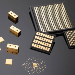
Designing a Printed Circuit Board takes more than connecting components. It is a balance of logic, structure, and creativity. A clever layout can keep devices running smoothly instead of buzzing with interference. For any PCB board manufacturer in Singapore, it’s the small design choices that make a big difference.
The Foundation of a Good Layout
A layout starts with a clear plan. Engineers decide how signals and power will move, keeping noisy components away from sensitive ones. The arrangement on screen becomes the skeleton of the real board.
A creative PCB layout company turns that schematic into an organised, workable layout. They choreograph how current moves, where copper layers overlap, and how each via connects the unseen pathways. The end goal is harmony between function and manufacturability.
Managing Power and Ground
Electricity has a mind of its own, so controlling its path is crucial. Narrow traces cause drops, and messy grounding invites noise. The secret lies in giving current a clear route to follow.
Within their process, a skilled PCB board manufacturer in Singapore balances copper thickness and spacing to manage power flow. Each layer is reviewed to ensure the board stays cool, steady, and safe under pressure.
The Importance of Component Placement
Good layout work is like arranging musicians in an orchestra. Each part has a role, and proximity matters. Heat-generating parts need breathing room, while signal processors prefer a quiet neighbourhood.
When a PCB layout company fine-tunes placement, it focuses on foresight and rhythm. Using simulation tools, designers map thermal zones and predict electromagnetic behaviour before production starts. It’s a design that listens as much as it leads.
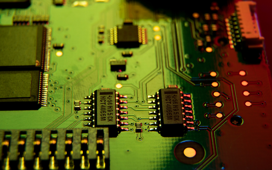
Traces: The Highways of Electricity
Traces are the lifelines of every PCB. They carry signals with the precision of well-marked roads. Width, spacing, and route all affect performance. Too close, and signals argue; too long, and they lag behind.
An experienced PCB board manufacturer in Singapore examines these routes like a traffic planner, checking impedance and avoiding signal jams. Clean routing keeps communication clear and circuits running without collisions.
Layering for Complex Designs
Complex circuits need room to breathe. Multiple layers create order from chaos, giving space for power, ground, and signals to live in harmony. Each layer brings structure and calm to a crowded board.
A forward-thinking PCB layout company decides how many layers a design needs, arranging them to balance space and signal clarity. Layer stacking, via positioning, and alignment all play their part in a steady and efficient performance.
Avoiding Heat and Interference Issues
Heat and noise are silent saboteurs in electronic design. Poor layout can trap heat and distort signals. Designers counter this with copper fills, thermal vias, and mindful spacing. In this stage, a PCB board manufacturer in Singapore checks every thermal path and grounding technique. They ensure that heat escapes efficiently and signals remain sharp. It’s quiet prevention rather than noisy repair.
PCB Design as a Craft
Every seasoned PCB layout company treats PCB design as both craft and calculation. Tools simulate outcomes, but intuition guides placement, spacing, and symmetry. Each revision moves the design closer to balance and reliability. PCB design blends art and science. It transforms a web of circuits into an efficient and durable product that looks as smart as it performs.
How Design Choices Shape Performance
Thoughtful design choices affect everything from signal clarity to assembly speed. Collaboration between engineers and the PCB layout company ensures no detail is left unchecked. The smallest tweak can mean smoother power delivery or cleaner communication. A layout’s success lies in its invisible logic. When it’s done right, users never notice; it simply works.
The Blueprint for Reliability
A strong PCB layout is like a good foundation: unseen but vital. It manages power, keeps noise at bay, and holds every component in harmony. Behind every dependable device is a board designed with care and precision. Contact MPN Tech to collaborate with a PCB board manufacturer in Singapore that blends creativity with engineering mastery for results you can trust.